
ARK Pixhawk Autopilot Bus Carrier
WARNING
PX4 does not manufacture this (or any) autopilot. Contact the manufacturer for hardware support or compliance issues.
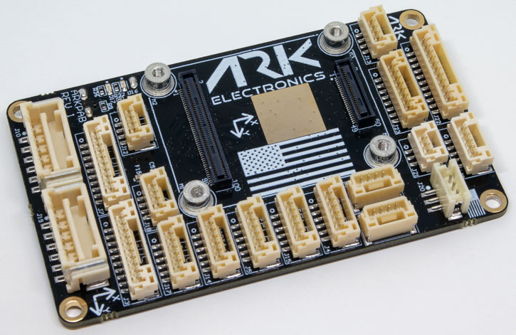
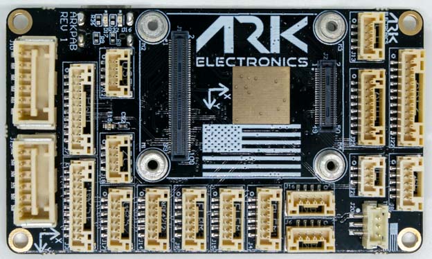
The ARK Pixhawk Autopilot Bus (PAB) Carrier is a USA-built flight controller carrier board, based on the Pixhawk Autopilot Bus open source standard.
The PAB form factor enables the ARK PAB Carrier to be used with any PAB-compatible flight controller, such as the ARKV6X.
Where To Buy
Order From Ark Electronics (US)
特性
连接器
- PAB Board to Board Interface
- 100 Pin Hirose DF40
- 50 Pin Hirose DF40
- Dual Digital Power Module Inputs
- 5V Input
- I2C Power Monitor
- 6 Pin Molex CLIK-Mate
- Ethernet
- 100Mbps
- Built in Magnetics
- 4 Pin JST-GH
- Full GPS Plus Safety Switch Port
- 10 Pin JST-GH
- Basic GPS Port
- 6 Pin JST-GH
- Dual CAN Ports
- 4 Pin JST-GH
- Triple Telemetry Ports with Flow Control
- 6 Pin JST-GH
- Eight PWM Outputs
- 10 Pin JST-GH
- UART/I2C Port
- 6 Pin JST-GH
- I2C Port
- 4 Pin JST-GH
- PPM RC Port
- 3 Pin JST-GH
- DSM RC Port
- 3 Pin JST-ZH
- SPI Port
- 11 Pin JST-GH
- ADIO Port
- 8 Pin JST-GH
- 调试接口
- 10 Pin JST-SH
尺寸
- Without Flight Controller Module
- 74.0mm x 43.5mm x 12.0mm
- 22g
电源
- 5V input on
POWER1,POWER2,USB C, and theUSB JST-GHconnector- Input is prioritized in the following order: POWER1 > POWER2 > USB
USB Cand theUSB JST-GHare in parallel- Overvoltage protection at 5.8V
- Undervoltage protection at 3.9V
VDD_5V_HIPOWERandVDD_5V_PERIPHcan each provide a total of 1.5A across all the connectors
LEDS
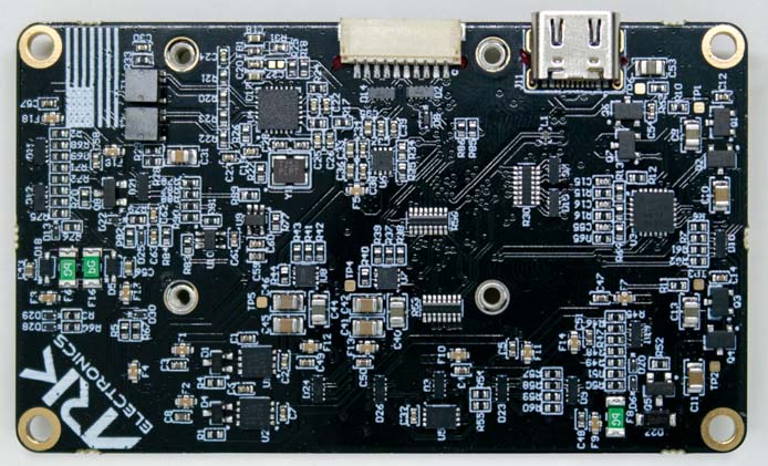
- There are two LEDs on the ARK PAB
Redis the ethernet power LEDGreenis the ethernet activity LED
针脚定义

POWER1
| 针脚 | 信号 | 电压 |
|---|---|---|
| 1(红) | VBRICK1 | +5.0V |
| 2 | VBRICK1 | +5.0V |
| 3 | I2C1_SCL | +3.3V |
| 4(黑) | I2C1_SDA | +3.3V |
| 6 | GND | GND |
| 6 | GND | GND |
POWER2
| 针脚 | 信号 | 电压 |
|---|---|---|
| 1(红) | VBRICK2 | +5.0V |
| 2 | VBRICK2 | +5.0V |
| 3 | I2C2_SCL | +3.3V |
| 4(黑) | I2C2_SDA | +3.3V |
| 6 | GND | GND |
| 6 | GND | GND |
PWM
| 针脚 | 信号 | 电压 |
|---|---|---|
| 1(红) | VDD_SERVO (Not Connected) | +5.0V |
| 2 | FMU_CH1 | +3.3V |
| 3 | FMU_CH2 | +3.3V |
| 4(黑) | FMU_CH3 | +3.3V |
| 6 | FMU_CH4 | +3.3V |
| 6 | FMU_CH5 | +3.3V |
| 7 | FMU_CH6 | +3.3V |
| 8 (blk) | FMU_CH7 | +3.3V |
| 9 (blk) | FMU_CH8 | +3.3V |
| 10 (blk) | GND | GND |
GPS1
| 针脚 | 信号 | 电压 |
|---|---|---|
| 1(红) | VDD_5V_PERIPH | +5.0V |
| 2 | USART1_TX_GPS1 | +3.3V |
| 3 | USART1_RX_GPS1 | +3.3V |
| 4(黑) | I2C1_SCL | +3.3V |
| 6 | I2C1_SDA | +3.3V |
| 6 | nSAFETY_SWITCH_IN | +3.3V |
| 7 | nSAFETY_SWITCH_LED_OUT | +3.3V |
| 8 (blk) | 3V3_FMU | +3.3V |
| 9 (blk) | BUZZER | +5.0V |
| 10 (blk) | GND | GND |
GPS2
| 针脚 | 信号 | 电压 |
|---|---|---|
| 1(红) | VDD_5V_HIPOWER | +5.0V |
| 2 | UART8_TX_GPS2 | +3.3V |
| 3 | UART8_RX_GPS2 | +3.3V |
| 4(黑) | I2C2_SCL | +3.3V |
| 6 | I2C2_SDA | +3.3V |
| 6 | GND | GND |
TELEM1
| 针脚 | 信号 | 电压 |
|---|---|---|
| 1(红) | VDD_5V_HIPOWER | +5.0V |
| 2 | UART7_TX | +3.3V |
| 3 | UART7_RX | +3.3V |
| 4(黑) | UART7_CTS | +3.3V |
| 6 | UART7_RTS | +3.3V |
| 6 | GND | GND |
TELEM2
| 针脚 | 信号 | 电压 |
|---|---|---|
| 1(红) | VDD_5V_PERIPH | +5.0V |
| 2 | UART5_TX | +3.3V |
| 3 | UART5_RX | +3.3V |
| 4(黑) | UART5_CTS | +3.3V |
| 6 | UART5_RTS | +3.3V |
| 6 | GND | GND |
TELEM3
| 针脚 | 信号 | 电压 |
|---|---|---|
| 1(红) | VDD_5V_HIPOWER | +5.0V |
| 2 | USART2_TX | +3.3V |
| 3 | USART2_RX | +3.3V |
| 4(黑) | USART2_CTS | +3.3V |
| 6 | USART2_RTS | +3.3V |
| 6 | GND | GND |
UART4/I2C3
| 针脚 | 信号 | 电压 |
|---|---|---|
| 1(红) | VDD_5V_PERIPH | +5.0V |
| 2 | UART4_TX | +3.3V |
| 3 | UART4_RX | +3.3V |
| 4(黑) | I2C3_SCL | +3.3V |
| 6 | I2C3_SDA | +3.3V |
| 6 | GND | GND |
I2C3
| 针脚 | 信号 | 电压 |
|---|---|---|
| 1(红) | VDD_5V_PERIPH | +5.0V |
| 2 | I2C3_SCL | +3.3V |
| 3 | I2C3_SDA | +3.3V |
| 4(黑) | GND | GND |
CAN1
| 针脚 | 信号 | 电压 |
|---|---|---|
| 1(红) | VDD_5V_HIPOWER | +5.0V |
| 2 | CAN1_H | +3.3V |
| 3 | CAN1_L | +3.3V |
| 4(黑) | GND | GND |
CAN2
| 针脚 | 信号 | 电压 |
|---|---|---|
| 1(红) | VDD_5V_PERIPH | +5.0V |
| 2 | CAN2_H | +3.3V |
| 3 | CAN2_L | +3.3V |
| 4(黑) | GND | GND |
USB
All signals in parallel with USB C connector
| 针脚 | 信号 | 电压 |
|---|---|---|
| 1(红) | VBUS_IN | +5.0V |
| 2 | USB_N | +3.3V |
| 3 | USB_P | +3.3V |
| 4(黑) | GND | GND |
ETH
| 针脚 | 信号 | 电压 |
|---|---|---|
| 1(红) | ETH_RD_N | +50.0V Tolerant |
| 2 | ETH_RD_P | +50.0V Tolerant |
| 3 | ETH_TD_N | +50.0V Tolerant |
| 4(黑) | ETH_TD_P | +50.0V Tolerant |
ADIO
| 针脚 | 信号 | 电压 |
|---|---|---|
| 1(红) | VDD_5V_PERIPH | +5.0V |
| 2 | FMU_CAP | +3.3V |
| 3 | BOOTLOADER | +3.3V |
| 4(黑) | FMU_RST_REQ | +3.3V |
| 6 | nARMED | +3.3V |
| 6 | ADC1_3V3 | +3.3V |
| 7 | ADC1_6V6 | +3.3V |
| 8 (blk) | GND | GND |
RC/SBUS
| 针脚 | 信号 | 电压 |
|---|---|---|
| 1(红) | VDD_5V_SBUS_RC | +5.0V |
| 2 | USART6_RX_SBUS_IN | +3.3V |
| 3 | USART6_TX | +3.3V |
| 4(黑) | VDD_3V3_SPEKTRUM | +3.3V |
| 6 | GND | GND |
PPM
| 针脚 | 信号 | 电压 |
|---|---|---|
| 1(红) | VDD_5V_PPM_RC | +5.0V |
| 2 | DSM_INPUT/FMU_PPM_INPUT | +3.3V |
| 3 | GND | GND |
DSM
| 针脚 | 信号 | 电压 |
|---|---|---|
| 1(红) | VDD_3V3_SPEKTRUM | +3.3V |
| 2 | GND | GND |
| 3 | DSM_INPUT/FMU_PPM_INPUT | +3.3V |
SPI6
| 针脚 | 信号 | 电压 |
|---|---|---|
| 1(红) | VDD_5V_PERIPH | +5.0V |
| 2 | SPI6_SCK | +3.3V |
| 3 | SPI6_MISO | +3.3V |
| 4(黑) | SPI6_MOSI | +3.3V |
| 6 | SPI6_nCS1 | +3.3V |
| 6 | SPI6_nCS2 | +3.3V |
| 7 | SPIX_nSYNC | +3.3V |
| 8 (blk) | SPI6_DRDY1 | +3.3V |
| 9 (blk) | SPI6_DRDY2 | +3.3V |
| 10 (blk) | SPI6_nRESET | +3.3V |
| 11 (blk) | GND | GND |
调试接口
The PX4 System Console and SWD interface run on the FMU Debug port.
The pinouts and connector comply with the Pixhawk Debug Full interface defined in the Pixhawk Connector Standard interface (JST SM10B connector).
| 针脚 | 信号 | 电压 |
|---|---|---|
| 1(红) | Vtref | +3.3V |
| 2 | Console TX (OUT) | +3.3V |
| 3 | Console RX (IN) | +3.3V |
| 4(黑) | SWDIO | +3.3V |
| 6 | SWCLK | +3.3V |
| 6 | SWO | +3.3V |
| 7 | NFC GPIO | +3.3V |
| 8 (blk) | PH11 | +3.3V |
| 9 (blk) | nRST | +3.3V |
| 10 (blk) | GND | GND |
For information about using this port see:
- SWD Debug Port
- PX4 System Console (Note, the FMU console maps to USART3).
另见
- ARK Pixhawk Autopilot Bus Carrier (ARK Docs)